
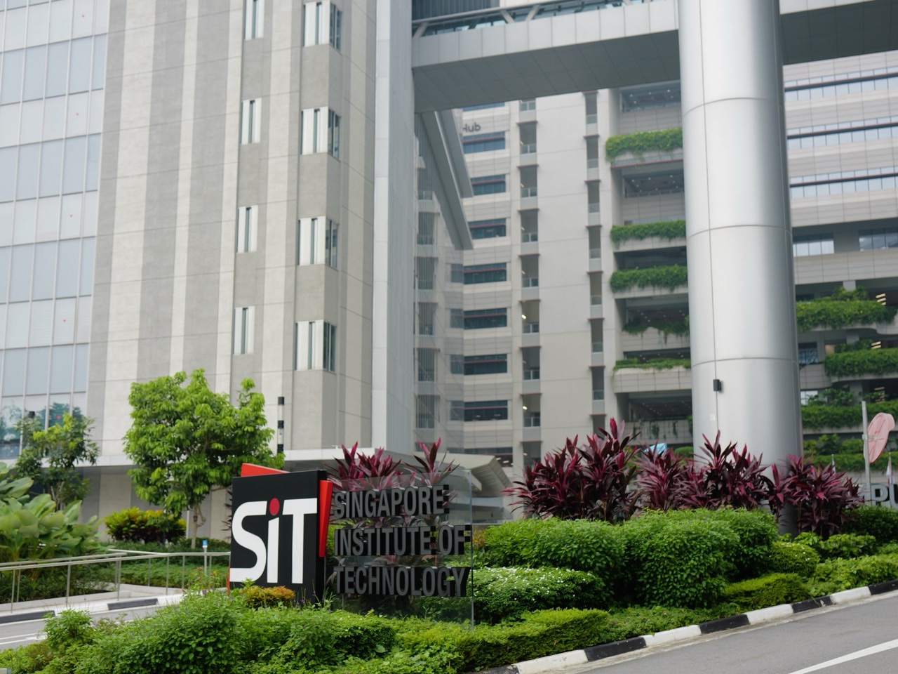
Quick answer, fact-checked 23 October 2026. SITLEARN at the Singapore Institute of Technology lists a Semiconductor Manufacturing and Process Control competency-based stackable micro-credential starting 4 January 2027 and ending 11 April 2027. Teaching is blended, with self-directed online learning, scheduled live sessions and in-person activities or assessments at SIT Punggol Campus, 1 Punggol Coast Road. SIT’s published application deadline is 23 November 2026, 11.59 pm. The full fee is S$10,006.20 including GST, with funding examples subject to eligibility and a separate S$54.50 one-time non-refundable matriculation fee.
This is not a new primary school, public science fair or automatically conferred engineering degree. It is a professional learning pathway comprising three credit-bearing modules: Semiconductor Process Integration (6 credits), Nanoscale Device Fabrication Technology (6 credits), and Process Risk and Yield Management (6 credits). A learner satisfying attendance and all required assessments may earn a Specialist Certificate that can contribute to selected further degree pathways under SIT’s academic rules. The official SIT course page is the primary source for all programme, deadline and fee details.
Punggol’s emerging university and technology district provides a useful backdrop for this kind of education. Semiconductor manufacturing is a specialised field that brings Chemistry, Physics, Mathematics, engineering processes, quality control and data analysis together. Families can use the news to explain why secondary-school fundamentals lead to advanced technological work, but an adult micro-credential should not be marketed as a course for children. This article gives parents and working professionals distinct routes through the information, labels worked examples as fictional, and separates a planned intake from any promise of admission or employment.
The January 2027 intake: facts first
- Programme: Semiconductor Manufacturing and Process Control, a competency-based stackable micro-credential delivered by SITLEARN.
- Published run: 4 January–11 April 2027, more than three months, blended online and on-campus.
- Application deadline: 23 November 2026 at 23:59, subject to provider updates.
- Campus: Singapore Institute of Technology, Punggol Campus, 1 Punggol Coast Road, Singapore 828608.
- Modules: ENG3201C Process Integration; ENG3202C Nanoscale Device Fabrication Technology; ENG3203C Process Risk and Yield Management, six credits each.
- Full published fee: S$10,006.20. After-funding illustrations: S$3,001.86 for eligible Singapore Citizens below forty and eligible PR/LTVP+ holders, S$1,165.86 for eligible Singapore Citizens forty and above.
- Additional charge: one-time non-refundable matriculation fee of S$54.50.
- Outcome: Specialist Certificate subject to at least 75% attendance and all credit-bearing assessments being passed.
- Action: review the live course page and official Apply Now link; an expression of interest does not guarantee admission.
Who is the intended learner?
SIT names prospective and existing semiconductor-industry professionals, including people interested in wafer fabrication, process and equipment engineering, product engineering, quality assurance, yield enhancement and research or development. The provider assumes foundational Physics, Chemistry and Mathematics, together with familiarity with semiconductor devices and fabrication through previous study or relevant experience. These prerequisites are not interchangeable with enthusiasm about computer chips. A learner should honestly compare their prior knowledge with the actual technical demands.
A professional already working in a wafer fab may want to formalise process-control methods, understand nanoscale device technology more deeply or build toward a recognised engineering qualification. A graduate from an adjacent engineering discipline might need to bridge knowledge of fabrication sequences and measurement techniques. Someone without an engineering base should first ask what introductory education would make this advanced curriculum suitable. Living close to the Punggol campus does not remove the need to meet the provider’s academic or experience criteria.
Why semiconductors are part of future education
Modern electronics depend on semiconductor devices. They appear inside processors, sensors, communications equipment, medical instruments, industrial controls and power-management systems. A semiconductor device is not simply ‘a chip’; it can be an individual component or part of a complex integrated circuit. Fabrication requires repeated processing of materials at very small scales under controlled conditions. The process demands precision not because the industry wants impressive terminology, but because small physical differences can affect electrical behaviour and reliability.
The subject gives students a concrete reason to study scientific ideas that might otherwise feel disconnected. Algebra and graphs help engineers analyse quantities and trends. Physics explains charge transport and device behaviour. Chemistry contributes knowledge of materials and processing. Statistics helps separate ordinary variation from signals of a problem. Technical English is essential for recording test results, explaining limitations and coordinating people working on interdependent steps. These connections support education, but they do not imply that every secondary pupil should pursue semiconductor manufacturing.
Module one: ENG3201C Semiconductor Process Integration
Process integration concerns how fabrication steps work together to produce a functioning device. A semiconductor is not manufactured by one magical machine. Material preparation, pattern definition, deposition, removal, doping, thermal steps and testing must be coordinated according to an engineered flow. Changing one step can alter the outcome of a later step, even when that later step is operating according to its own specification. The integrator therefore considers the entire process rather than optimising each stage independently.
A useful analogy is baking a layered product: ingredients, mixing, heating and cooling must be coordinated, and a variation early in the process may become visible only at the end. The analogy is limited because semiconductor fabrication requires far more precise equipment and material conditions. The correct lesson is the dependence of a finished outcome on an ordered sequence of controlled steps. It is not permission to attempt semiconductor processing at home or in a normal school science room.
The programme includes CMOS technology and its evolution, together with integration methods relevant to semiconductor devices. CMOS describes a family of complementary metal–oxide–semiconductor technologies used extensively in integrated circuits. A reader should distinguish this technical platform from the broad consumer label ‘computer chip’. The design and manufacturing route for a memory device, a sensor or a specialised photonic component may involve different processes and performance priorities.
Module two: ENG3202C Nanoscale Device Fabrication Technology
The second module deals with how very small structures are fabricated and measured. Nanoscale engineering requires sophisticated equipment, controlled environments and validated measurement. It is not enough to say a device is ‘tiny’; the relevant dimensions and uncertainties must be understood. When process steps operate on small features, contamination, alignment, material properties and measurement accuracy become critical. Professionals need to ask what a given tool actually measures and how trustworthy its result is.
SIT refers to advanced fabrication techniques, metrology and inspection tools. Metrology is the practice of measurement with defined standards and uncertainty. Inspection can reveal a defect or pattern requiring attention, but an observed anomaly does not automatically identify its cause. The learner should understand the difference between detecting a deviation, investigating the mechanism behind it and deciding whether a corrective process change is justified.
School pupils can learn the idea of scale using ordinary measurements: a millimetre is one-thousandth of a metre; a micrometre is one-millionth; a nanometre is one-billionth. However, this conceptual exercise must not be turned into a claim that a child’s ruler can resolve the same features as specialised semiconductor instruments. The purpose is to learn what the units mean and why precision requires appropriate tools, not to imitate professional laboratory methods with unsuitable equipment.
Module three: ENG3203C Process Risk and Yield Management
Yield describes the proportion of manufactured outputs meeting a defined acceptance criterion. It matters because making many components does not provide value if a large fraction is unsuitable for the intended use. Yield management combines data, careful definitions, process understanding and corrective action. The same numerical yield figure can mean different things when acceptance tests, product types or sampling conditions differ. Good analysis first establishes what was counted and why.
Process risk management asks what could go wrong, how serious the consequences would be, how likely a failure is under relevant conditions, and how problems could be prevented or detected. In a complicated fabrication flow, different failure mechanisms may interact. A hurried change intended to improve throughput can increase defects; a stricter inspection can identify more defects without the underlying manufacturing quality becoming worse. Metrics must be interpreted in context.
SIT says learners will encounter process optimisation, statistical process control, risk analysis and yield management. These are professional tools rather than buzzwords. Their value depends on the user’s ability to explain assumptions, investigate unexpected results and treat evidence responsibly. A classroom formula does not authorise changes to an actual production line; approved procedures, supervision and the employer’s safety rules remain essential.
Worked Mathematics: a basic yield calculation
Suppose a hypothetical exercise produces 1,000 devices and 930 pass a defined test. The observed yield is 930 ÷ 1,000 × 100% = 93%. If a later batch of 1,200 devices has 1,128 passes, yield is 1,128 ÷ 1,200 = 94%. Comparing only the number of passes—930 versus 1,128—would hide the fact that the second batch was larger. Comparing percentages is more informative when the tests and populations are genuinely comparable.
The difference between 93% and 94% is one percentage point, not a one-percent relative increase. Relative to 93%, the increase is approximately 1 ÷ 93 = 1.08%. These two statements answer different questions. Engineers and managers should be precise about which is intended. The fictional example teaches percent and ratio reasoning; it does not report any real fab’s yield or suggest that one percentage point always has the same economic significance.
If the second batch uses a more lenient pass criterion, the higher yield may reflect the rule rather than improved fabrication. If the product mix changed, a comparison may be unfair. A professional investigator checks the definition of a passing device, the test method, sample and operating conditions before making a claim. A higher number is not automatically evidence of better engineering. The quality of the inference depends on the quality of the measurement system.
Worked Mathematics: defects per batch
A fictional inspection finds 20 defects in a batch of 500 devices and 24 defects in a batch of 800. The observed defects per device are 20 ÷ 500 = 0.04 and 24 ÷ 800 = 0.03 respectively. The raw defect count rises from 20 to 24, while the normalized rate falls from 4% to 3% in this simplified exercise. A manager who uses only counts may reach the wrong conclusion about the change.
This rate calculation assumes one counted defect per failing device or another clearly specified counting rule. Real defect data can include multiple defects per device, different severities and varied detection sensitivity. The unit and definition must be printed on every serious analysis. A graph labelled ‘defects’ without a denominator or inspection boundary is too vague to justify a production decision. The numerical example is intentionally simple so learners focus on the meaning of the calculation rather than an advanced statistical technique.
A short introduction to statistical process control
Statistical process control uses structured data to identify patterns that may deserve investigation. Not every up-and-down movement is an abnormal event: even a stable process has some natural variation. Conversely, an unusual run or trend may indicate that something has changed. A professional needs suitable measures, enough relevant observations and appropriate interpretation. The aim is not to punish staff whenever a graph moves but to improve understanding of the process.
For a classroom thought experiment, imagine five measurements of a fictional dimension: 10.1, 9.9, 10.0, 10.2 and 9.8 units. Their mean is 10.0. That calculation does not establish whether the process meets an engineering tolerance, whether the instrument is calibrated or whether the variation is acceptable. The learner should explicitly ask for the specification and measurement uncertainty. Mathematics supplies the mean; engineering requires more evidence to decide what it means.
Control limits and product specifications are also different ideas. A process may be statistically stable but consistently produce outside the required specification. Conversely, all observed items may lie within specifications even while the process shows a pattern that warrants investigation. These distinctions are advanced but useful: a manager who confuses ‘within our recent normal range’ with ‘meets customer requirements’ may make a serious mistake.
What does risk assessment change?
A professional risk assessment examines failure modes and consequences before or during decisions. Imagine a fictional measurement sensor occasionally reporting an incorrect value. One possible consequence is a mistaken process adjustment; another is an unnecessary stop. The relevant response depends on what the sensor controls and whether independent checks exist. The most dramatic imagined consequence is not automatically the most probable, but a rare severe risk may still need strong safeguards.
A student should learn to separate hazard, exposure, likelihood and consequence rather than use the single label ‘dangerous’. A well-designed system might prevent an inappropriate action, detect a deviation and provide a safe fallback. Those are different protective functions. This reasoning connects semiconductor process control with broader fields such as healthcare, transport and information security. It also encourages clear reporting when uncertainty remains.
How the course is organised across three months
SIT’s published schedule lists an in-person initial briefing, self-directed learning across weeks 1–12, Friday evening online consultation sessions from 7 to 10 pm, and selected in-person laboratories and assessments. Laboratory sessions are named for weeks 8, 10 and 11, with course assessments during specified weeks and an in-lab project assessment in week 13. Some assessment times remain to be confirmed. A blended course is not an entirely self-paced programme without any fixed commitments.
This matters to a working parent. Even if recorded content can be studied flexibly, scheduled online consultations and on-campus assessments require real time. People working shifts or caring for children should map the entire calendar before accepting a place. A fictional plan assuming ‘three months online’ can fail when laboratory days, travel and assessment preparation are added. The responsible question is which sessions are compulsory and what arrangements SIT allows if a learner’s work schedule changes.
A learner should also reserve time for reading, writing and correction. An hour listed on a timetable may not represent an hour of total work. Preparing a report, practising statistics and solving an unfamiliar problem independently can take longer. Protecting a sustainable routine through April 2027 is more valuable than planning a heroic first week that cannot be maintained. The formal course team is the authority for workload expectations and support options.
Who teaches, and what is the learning approach?
SIT’s named teaching team includes engineering faculty and educators with semiconductor and electronics experience, including an Associate Professor in engineering, a lecturer from Republic Polytechnic and an engineer-scholar in circuits and systems. The course is described as competency-based: the learner is expected to demonstrate relevant knowledge and skill rather than merely accumulate classroom hours. The public listing discusses written examinations and reports, with success coaching available to support learning strategy.
The value of this approach is greatest when feedback identifies how a conclusion was reached. A report that says ‘yield increased’ without defining a baseline, test or confidence in the data may look impressive but explain little. A stronger report shows the measure, conditions, possible alternative explanations and a justified next check. This habit can be taught much earlier in school, but professional practice requires more advanced knowledge and responsibility.
Fees and subsidies: separate published tables from approval
SIT’s full listed fee is S$10,006.20 including GST. Its published after-funding examples are S$3,001.86 for eligible Singapore Citizens below forty and eligible Singapore PR/LTVP+ learners, and S$1,165.86 for eligible Singapore Citizens forty and above under the stated enhanced scheme. A non-Singapore Citizen in the non-funded category is shown the full amount. SIT also lists a one-time, non-refundable matriculation fee of S$54.50. These are published illustrations, not guarantees about an individual’s invoice.
The exact amount payable depends on current eligibility and approvals. A learner should not treat being over forty as sufficient to establish every benefit. Funding schemes can distinguish course-fee subsidies, SkillsFuture Credit and other support. An employer may also sponsor some expense under separate arrangements. Ask the provider for an itemised, current quotation and identify which support has actually been approved rather than subtracting hypothetical grants from a household budget.
The S$300 monthly allowance is conditional
SIT’s page explains that some eligible Singapore Citizens aged at least forty who satisfy recent in-employment conditions may apply for a part-time SkillsFuture Mid-Career Training Allowance of S$300 a month during an eligible course. The application requires official approval and includes attendance-related conditions. This allowance is not automatic, and it is separate from a tuition subsidy. A reader should check the live SkillsFuture portal and provider terms for individual eligibility.
If a household relies on a possible allowance to pay bills, it risks budgeting money that may not be approved or may arrive under a different schedule. A safer plan uses confirmed funds for compulsory expenses and treats conditional support separately until the official decision exists. This is a general personal-budgeting principle, not a claim about how any particular applicant’s finances work. Course participation should remain feasible even when assumptions about financial support are corrected.
Is the Specialist Certificate the same as a degree?
No. SIT describes a credit-bearing micro-credential leading to a Specialist Certificate after completing all relevant assessments and attendance conditions. It is one possible component of a longer Competency-based Stackable Micro-credential Pathway. The page names possible progression toward engineering degrees and an Integrated Studies technology-and-management route under relevant criteria. This possibility is important, but it is not unconditional admission or automatic conversion into a completed bachelor’s qualification.
Each later route has its own recognition and entry requirements. SIT explains that moving formally into a degree pathway changes the applicable tuition and funding arrangements. SkillsFuture course-level subsidies are not simply carried into full-degree enrolment, and the learner must check degree costs and any eligible MOE Tuition Grant separately. A credible education plan therefore considers both the value of the standalone certificate and the extra commitment involved in stacking toward a degree.
Prospective students should ask SIT how long their earned credits remain valid, what other micro-credentials are required, and whether previous diploma or work experience can be assessed through Recognition of Prior Learning. The broad pathway site says certificates and credits are valid for a stated period for stacking and that entry rules differ across courses. Do not assume that every module transfers to every degree or that enrolment in a micro-credential fixes all later conditions.
Why this development does not guarantee semiconductor jobs in Punggol
A university teaching semiconductor manufacturing at Punggol does not establish that a new chip-fabrication plant is opening in the neighbourhood or that students will be assigned to a particular employer. The programme draws on a nationally important technical domain. Graduates may work in many locations and industries, with employment dependent on experience, qualifications, current vacancies and individual recruitment processes. A geographical education connection is not a promise of local factory capacity.
The practical benefit of locating applied learning in Punggol is that residents can see and access a university-level training environment as part of Singapore’s broader education ecosystem. Companies may value staff who strengthen process-control and metrology competencies, but each employer decides whether an applicant’s skills fit a job. Parents should encourage genuine science learning rather than tell a teenager that one technical field guarantees high pay or long-term certainty.
What Secondary students can learn from the announcement
A Secondary 1 student should not begin by memorising nanoscale process acronyms. Their first tasks are accurate fractions, ratio, units, graph interpretation and the ability to solve and check equations. A Secondary 3 student taking appropriate Science and Mathematics might study the semiconductor conceptually through energy bands, circuit behaviour or materials, according to their actual syllabus. Advanced fabrication is a future specialisation, not a requirement for every pupil.
The teaching approach from eduKate’s Secondary 1 Mathematics exemplar is relevant: if a student mistakes a percentage-point change for a percentage change, correct the underlying reasoning before asking them to interpret an engineering chart. A tiny numerical misunderstanding can scale into a large error in a professional report. Precision in the fundamentals is a valuable form of future preparation, even for a student who ultimately chooses a different field.
English matters too. Engineers document methods, interpret specifications, write investigation findings and communicate uncertain conclusions. A professional statement such as ‘the batch yield was lower under these test conditions; further checks are needed’ is different from declaring that a specific technician caused a defect. Clear writing helps an organisation distinguish observation, inference and action. Children can practise those distinctions in scientific reports long before entering industry.
A safe home learning example: materials and conduction
A child can compare familiar descriptions of conductors and insulators using approved school materials and safe low-voltage demonstrations led by a teacher. Semiconductors deserve their own explanation because their electrical behaviour can be influenced through material properties and device design. Do not imply that touching a silicon-like household object reveals the way a nanoscale device operates. Classroom inquiry should begin with definitions, diagrams and trusted educational materials rather than attempting chemical processing or high-temperature experiments.
Professional fabrication may involve hazardous chemicals, high temperatures, vacuum equipment and regulated workplace procedures. No part of an adult micro-credential announcement permits a family to improvise wafer cleaning, etching or deposition in a kitchen or classroom. A safe education guide keeps specialist manufacturing details conceptual and encourages learners to use institutional laboratories only with proper supervision and authorisation.
Independent practice: ratios and yield
- A: 360 of 400 fictional components pass a test. Find the yield percentage.
- B: 570 of 600 components pass. Which batch has the higher observed yield?
- C: a pass rate rises from 90% to 95%. State the percentage-point change.
- D: a lab reports five measurements: 10, 12, 11, 9 and 8 units. Find the mean.
- E: explain why a better yield figure alone cannot establish which fabrication process is safer or more reliable.
Answers: A = 360 ÷ 400 × 100% = 90%. B = 570 ÷ 600 × 100% = 95%, higher than A. C = five percentage points. D = (10 + 12 + 11 + 9 + 8) ÷ 5 = 10 units. E requires discussing comparable tests, product types, reliability, safety and measurement quality. The questions are original classroom practice, not actual SIT assessment questions or manufacturing measurements.
A realistic 2026–2027 planning sequence
- Now: read the full SIT entry criteria and identify which prior engineering knowledge you have.
- Before 23 November 2026: verify the application deadline, course run and personal fee quotation.
- Before accepting a place: inspect Friday online-session commitments, laboratory weeks and assessment dates.
- During December 2026: revise relevant Mathematics, Chemistry, Physics and statistical reasoning where weak.
- From 4 January 2027: follow the provider’s formal blended-learning schedule and preserve authorised records.
- During laboratory and assessment weeks: protect time for transport, preparation and safe supervised work.
- After the 11 April 2027 scheduled end: retain assessed work permitted by SIT and evaluate any further degree route separately.
Frequently asked questions
When does the next listed semiconductor micro-credential begin?
The provider lists 4 January 2027 through 11 April 2027, with blended delivery centred on the SIT Punggol Campus. Dates and activity times should be confirmed through the live portal and accepted joining instructions.
When is the January 2027 application deadline?
SIT’s public programme page lists 23 November 2026 at 23:59. A submitted form is not proof of accepted admission, and a current application button does not guarantee places remain.
Can Primary or secondary-school students attend?
It is designed for people preparing for or working in semiconductor manufacturing and assumes relevant technical foundations. Children can learn supporting science and mathematics at the proper school level but should not regard this as a children’s course.
Is the course fully online?
No. The schedule combines self-directed online content, live online consultations and specified in-person laboratory and assessment activity. Exact reporting requirements belong to the provider.
Does completing the course automatically award a degree?
No. It leads to a Specialist Certificate if the conditions are satisfied and may contribute toward selected degree pathways under additional academic and financial requirements.
Will every applicant aged forty or above receive S$1,165.86 pricing?
Not automatically. The figure is for the relevant funding category subject to eligibility and official approval. Additional fees and later degree costs must be considered separately.
Is a monthly training allowance guaranteed?
No. SIT describes conditional support for eligible mid-career learners who meet employment-history and attendance rules and receive SkillsFuture approval.
Does the course involve access to a commercial wafer fab?
The public schedule names in-person laboratory sessions and assessments at SIT. It does not give visitors an unrestricted right to enter industrial semiconductor sites. Do not invent employer-site visits or lab access arrangements.
Will semiconductor work necessarily be located in Punggol?
No such geographical job guarantee follows from the university programme. The course is an education opportunity delivered at Punggol, while employer location and hiring are separate facts.
A useful manufacturing distinction: throughput and yield. Suppose a fictional line processes 1,000 units per day with 90% of them passing, producing 900 good units. A different process handles 900 units with a 98% pass rate, producing 882 good units. The second process has the better pass percentage but the first produces more acceptable units under those simplified assumptions. Neither number proves which operation is preferable without considering costs, quality specifications, reliability and resources. A manager who focuses on only one metric may optimise the wrong outcome. This example shows how Mathematics and systems thinking meet semiconductor manufacturing.
Why equipment data needs context. A sensor might show a change in temperature, pressure or process duration, but one reading alone does not establish a defect mechanism. The learner should know how the sensor is calibrated, when the measurement was taken, whether the data belongs to the correct batch and how the process normally varies. If the measurement is inconsistent with other evidence, a careful investigator considers instrument error as well as a genuine process event. In critical manufacturing, the discipline of making uncertainty visible can prevent expensive or unsafe decisions. The exercise reinforces scientific method rather than an instruction for actual equipment troubleshooting.
Defects, quality and the limits of inspection. Catching more defects at the end of a process may protect customers but can increase the amount of rejected material. Preventing defects earlier may be a stronger long-term approach, provided its effects are verified. A professional needs to distinguish prevention, detection and recovery. If a company reports a dramatic increase in detected defects after introducing improved inspection, it may initially appear as though manufacturing became worse when the measurement system became more sensitive. The correct conclusion requires examining the change in detection procedure and the underlying process, not merely comparing counts.
Academic credit is not a blank cheque. The Specialist Certificate’s credit-bearing modules matter because learners may have opportunities to stack recognised study. But credits belong to formal rules about applicable programmes, validity periods, prerequisite knowledge and permitted progression. Before assuming that three modules have purchased part of a specific degree, ask SIT to identify the current route and any restrictions. A professional may choose to stop after one credential, which is a valid educational decision. The longer pathway should be considered when it adds meaningful career competence rather than because the first certificate creates pressure to continue spending.
Writing a trustworthy project reflection. A learner can use the structure question, method, evidence, result, limitations and next action. For a hypothetical yield study, the report might state what passed, what failed, how many devices were counted, whether conditions were comparable, and what further investigation is justified. Avoid making an unjustified claim about an employee or supplier from one dataset. Technical writing is valuable because it lets a second person examine the reasoning and find where it might fail. The strongest report does not hide uncertainty; it makes uncertainty manageable.
Six weeks after the course. A learner can revisit a fictional process problem without relying on slides. Compute a yield, identify a possible measurement bias, explain why inspection and prevention differ, and state what evidence would be needed before proposing a process change. If the person can transfer the method to a different set of numbers and conditions, the learning has become more durable. This reflection is complementary to formal assessment, not a replacement. Real production work remains governed by employer authorisations, trained supervision and applicable safety and quality systems.
Family learning without career pressure. A parent working in technical manufacturing may use a simple arithmetic example to show a child where ratios and graphs appear outside the classroom. The conversation should remain age-appropriate and should not disclose confidential employer processes. A child who prefers languages, arts or social sciences can still benefit from scientific literacy without being channelled into semiconductors. The educational value lies in understanding evidence and having genuine options, not in treating a local university programme as proof that one occupation is superior to all others.
Official sources and related Punggol articles
- SITLEARN — Semiconductor Manufacturing and Process Control: modules, dates, fees and degree pathways
- SIT — Competency-based Stackable Micro-credential Pathway, eligibility and recognition principles
- SIT — Electrical and Electronic Engineering micro-credentials and degree routes
- JTC — Punggol Digital District as a university-industry learning setting
- eduKatePunggol — January 2027 Operations Excellence micro-credential
- eduKatePunggol — adult skills and lifelong learning at SIT
- eduKatePunggol — November 2026 solar PV engineering course
Editorial fact-check, 23 October 2026: Programme dates, entry background, module codes, fees and study modes come from the official SITLEARN course page. Arithmetic and factory examples use invented values; they are not measurements from a Punggol semiconductor plant and are not professional manufacturing procedures. Individual admission, funding and credit recognition must be confirmed by SIT.


